Application of Micro/Nano Bubble Cleaning Technology in the Ultra-Clean Semiconductor Cleaning Field - Shanghai Zhongjing
Click:1461Date:2025-12-13 04:28:31
Shanghai Zhongjing Environmental Protection Technology Co., Ltd. is a modern enterprise integrating research and development, manufacturing, sales, and service, deeply cultivating the field of micro nano bubble technology. Its core technology adopts multiphase fluid vortex cutting and other processes, which can generate 10-100nm uniform bubbles, with advantages such as efficient mass transfer and strong oxidation. The product is suitable for multiple scenarios such as environmental protection, agriculture, industry, and biology. With the characteristics of intelligent regulation, safety, and stability, it provides green solutions for wastewater and waste gas treatment, crop quality improvement, etc., and has been recognized by many well-known enterprises and research institutions.
Shanghai Zhongjing Micro Nano Bubble Cleaning Technology is a new green technology in the field of semiconductor ultra clean cleaning. With its unique equipment structure and technical principles, it has significant advantages in cleaning effect, safety, and environmental protection, and is suitable for the cleaning needs of semiconductor device miniaturization and high precision. The following is a detailed introduction:
Core technology and equipment situation
Working principle: Its core is to use technologies such as gas-liquid shear force variation and multiphase fluid vortex cutting to highly fuse gases such as air, oxygen, and nitrogen with liquids through high-speed vortex cutting. Then, the bubbles in the gas-liquid mixture are chopped to 10-100nm to form high concentration micro nano bubble water. These bubbles carry negative charges and have both oxidizing and sterilizing effects when they self contract and explode. They can also generate an ultra-high pressure and high temperature reaction field through instantaneous adiabatic compression, helping to remove pollutants.
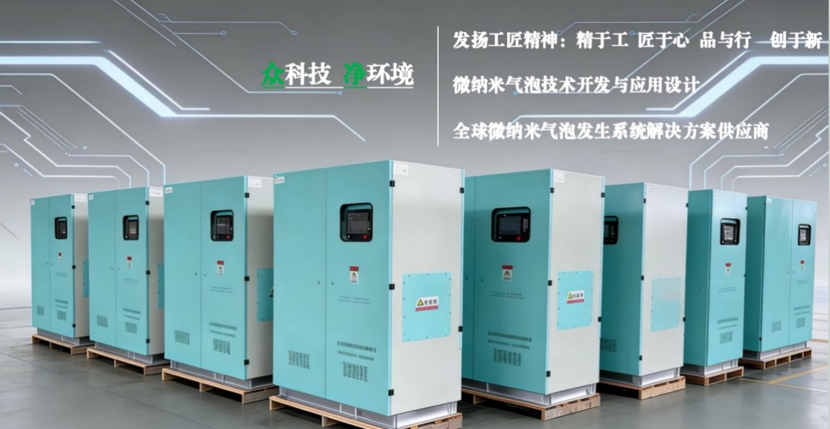
Equipment structure: The equipment consists of a mixing device, a rotary cutting device, a spraying device, and a control system, which need to be matched with supporting pipelines such as an intake pipeline and an inlet pipeline. The overcurrent components use non-metallic media and are equipped with a CPU integrated control system, which can monitor key parameters such as flow rate and water temperature in real time; And the liquid receiving part is made of non-metallic materials such as fluororesin to avoid metal ion contamination of semiconductor components. At the same time, the equipment is equipped with multiple safety protection mechanisms such as overvoltage and overheating to ensure continuous and stable operation.
Core advantages in semiconductor cleaning
Efficient and thorough cleaning: Micro nano bubbles have small volume and large specific surface area, which can easily penetrate into the tiny gaps and holes of semiconductor chips. By utilizing the high-frequency vibration caused by bubble movement and rupture, combined with the free radical reaction generated by bubble explosion, surface dust, oil stains, photoresist, metal pollutants, etc. can be efficiently removed. Compared with traditional methods, the cleaning time can be shortened from 5 minutes/cycle to 2 minutes/cycle, and the process time can be reduced by more than 1/4. For example, in the post manufacturing process of IC, this technology can significantly enhance the cleaning effect by cleaning in photoresist solvent solution.
Reduce the risk of component damage and contamination: When bubbles burst, the impact force is mild, which significantly reduces the risk of semiconductor component damage and improves the yield rate compared to traditional strong mechanical impact cleaning. Moreover, the cleaning process can avoid the use of harmful chemicals and solvents, reducing the corrosion and pollution of semiconductor components caused by chemical agents, and eliminating the need for complex spray and waste liquid treatment processes. For example, in the cleaning of compound semiconductor substrates after grinding, micro nano bubbles in acidic solutions can safely remove foreign objects and metal contamination.
Significantly reducing production costs: By not relying on a large amount of chemical agents, drug costs can be reduced by over 90%; Simultaneously simplifying the waste liquid treatment process, reducing waste liquid treatment costs by over 50%, significantly reducing the cost of cleaning in semiconductor manufacturing, and further improving production efficiency by enhancing cleaning efficiency and yield.
Suitable semiconductor cleaning scenarios
Suitable for alkaline solution scenarios, it can be used for organic stripping and cleaning of electronic product substrates, fixtures, etc;
Suitable for acidic solution scenarios, it can perform foreign object removal and metal contamination cleaning on compound semiconductor substrates, and can also be used for cleaning after semiconductor grinding;
Suitable for photoresist solvent scenarios and applied in post IC manufacturing processes, it can enhance the cleaning effect of glass components and ensure the smooth progress of subsequent semiconductor packaging and other processes.


 Home
Home


